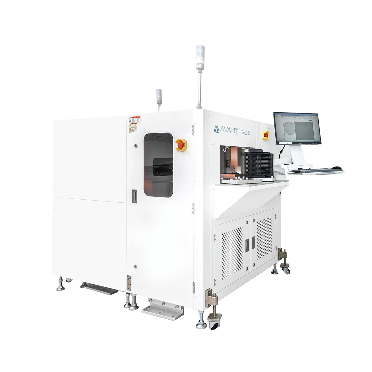
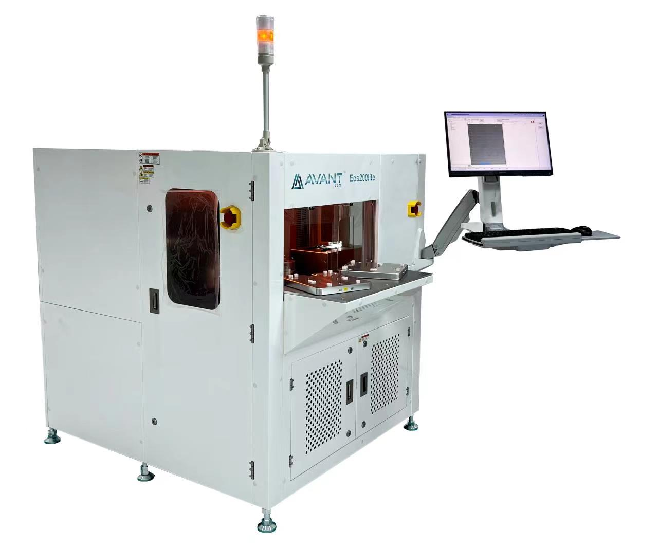
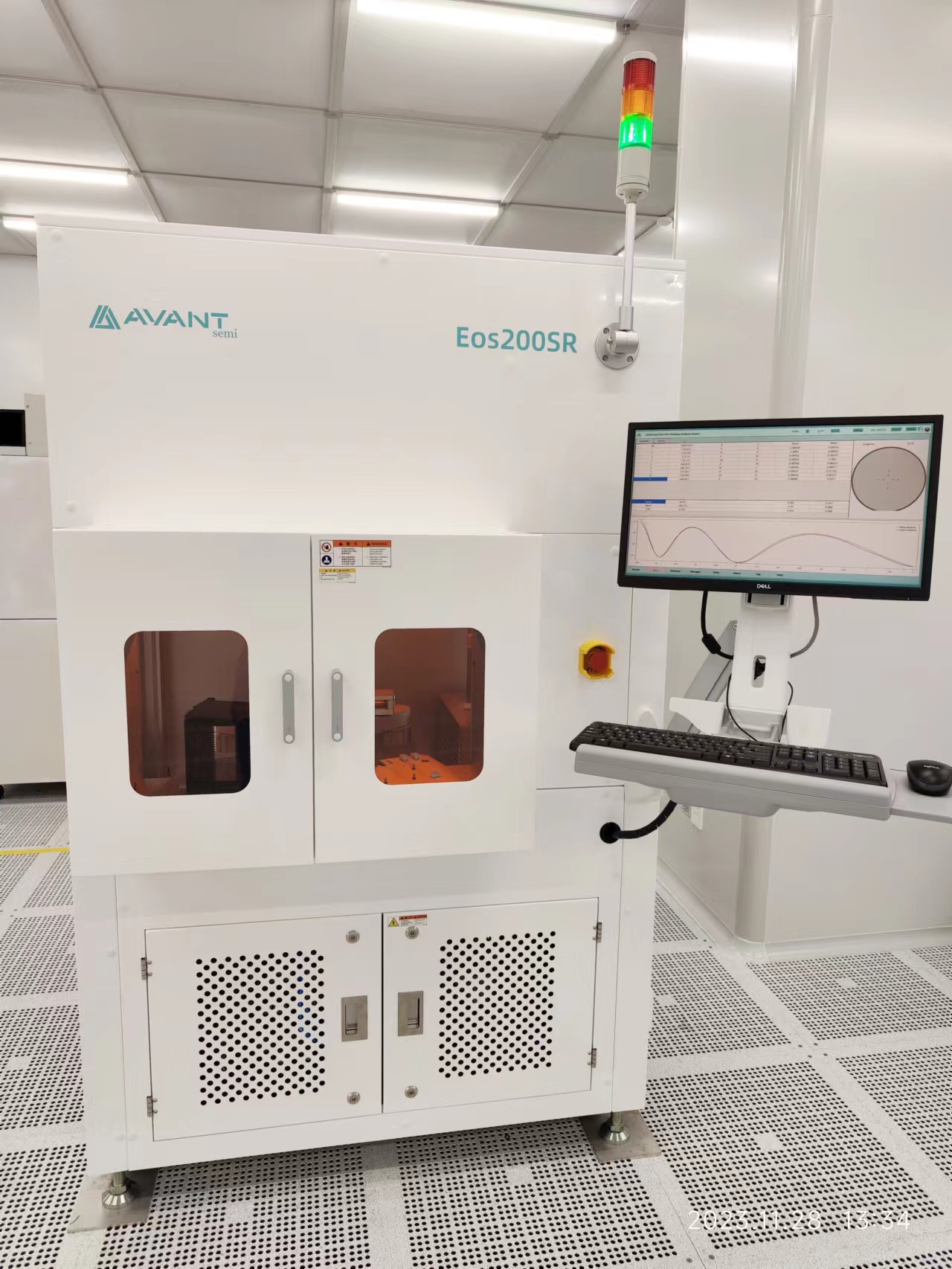
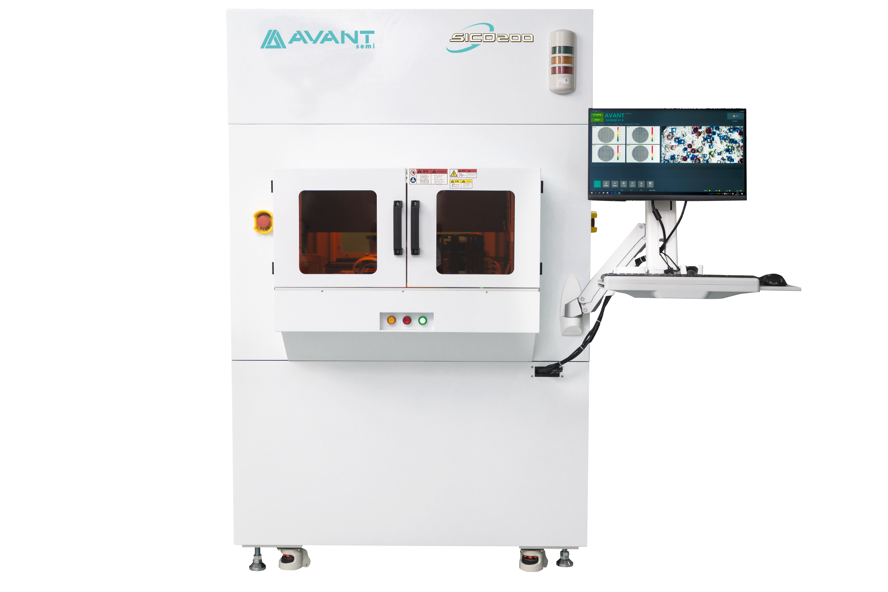
Avantsemi filled the gap of semiconductor front-end inspection & measurement equipment in China
Avantsemi was established in September 2021, the company is located in Shanghai Zhangjiang Hi-Tech Park.
Avantsemi was founded under the leadership of a returned overseas doctor who has long been engaged in the semiconductor industry and a domestic senior IC front-end process inspection & measurement equipment technical team. The team members have been deeply involved in the semiconductor front channel inspection & measurement equipment industry for a long time, and have deep industrial background, industrial resources and industrial chain resources of equipment manufacturing in China.
Adhering to the belief of seeking truth from facts and going far, adhering to the spirit of pragmatism and efficiency. Avantsemi is committed to building high-quality semiconductor front-end inspection & measurement equipment and contributing to filling the gap of semiconductor front-end inspection & measurement equipment in China. Meanwhile, technological innovation is realized on the basis of profound technological accumulation.