Recently, Shanghai Youruipu Semiconductor Equipment Co., Ltd. (hereinafter referred to as "Youruipu") successfully delivered a wafer edge inspection equipment SICE200 to customers, which can be used for edge defect detection of silicon-based and compound semiconductor substrates and epitaxial wafers.
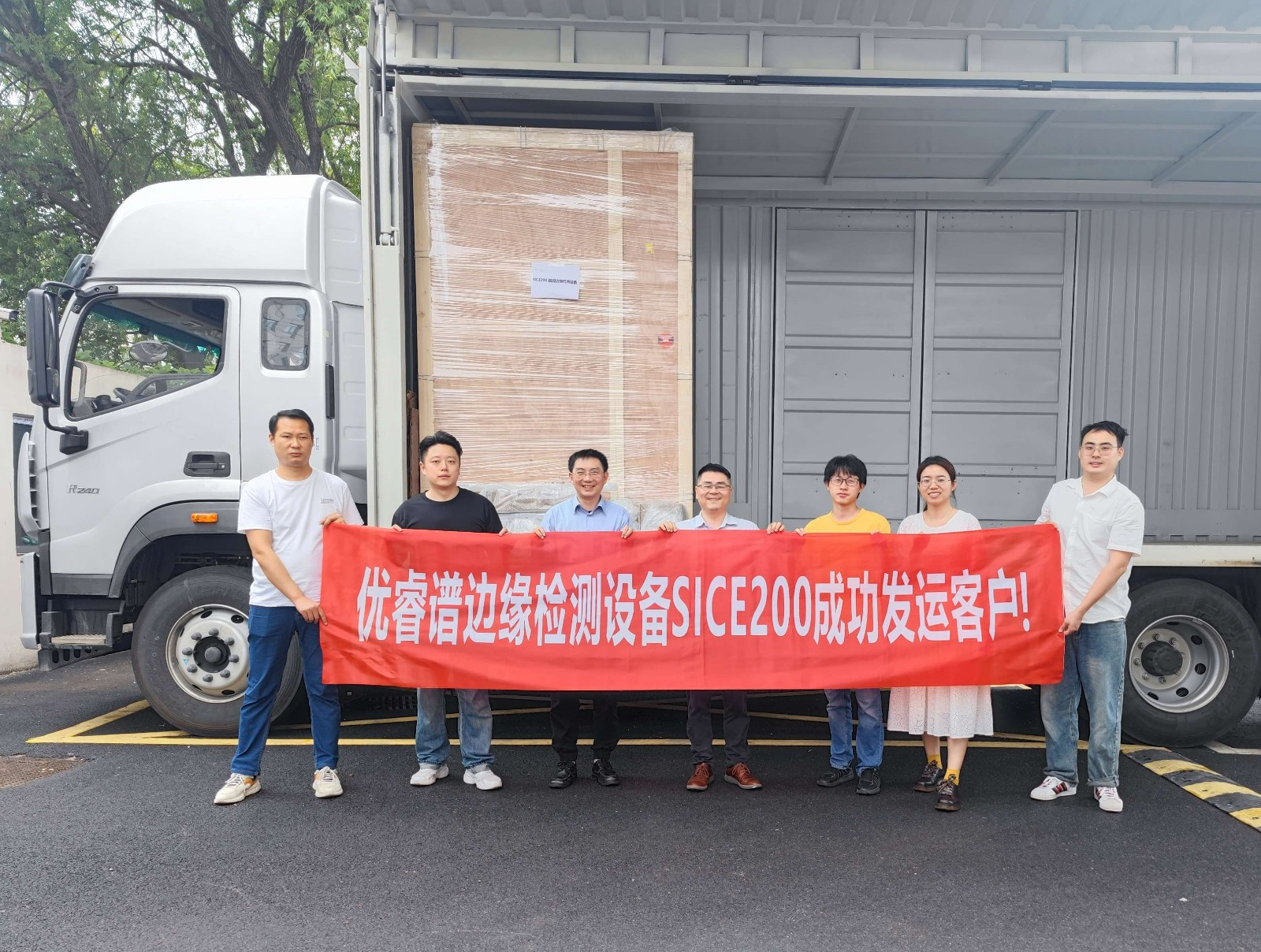
Figure 1: Unispectrum successfully delivered the customer's SICE200 equipment
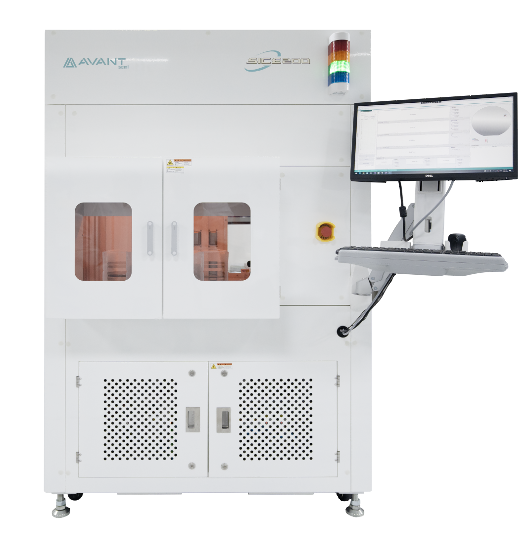
Figure 2: Picture of the appearance of the SICE200
According to Dr. Tang Deming, general manager of Uruipu, the SICE200 equipment launched by Uruipu this time has the following technical characteristics:
It is compatible with 6&8 inch SiC&Si substrates and epitaxial wafer edge inspection, and is also suitable for edge defect detection of other compound
substrates and epitaxial wafers
Simultaneous 360° inspection of wafers (defect inspection on the front, back, and edges of the wafer)
Simultaneous and accurate measurement of wafer chamfer and diameter (optional)
The opto-mechanical system with independent intellectual property rights can achieve high resolution, high detection rate and high detection rate
Wafer thickness, TTV/Warp/Bow and other parameters measurement (optional)
Dr. Tang Deming said that at the level of the whole machine software and defect detection algorithm, SICE200 has the following technical advantages:
Image enhancement technology: Highlight edge chipping, cracks, surface scratches, stains and other defect features
Abundant Condition Combination Judgment Parametric Detection Tools: A variety of high-precision detection algorithm tools, with a high degree
of adaptability, can accurately judge and identify defect categories, and accurately classify them
Wafer chamfering and diameter measurement technology: accurate measurement, fitting, calculation of chamfer and diameter dimensions of edge
contours and wafer diametersFunctional modularization: Modular inspection software functions, can quickly configure inspection programs (Recipes)
to meet customers' individual inspection needs (optional)
Defect Diagram: Data retention for Defect Review
Typical feature defect and chamfer measurements for SICE inspection

Figure 3: Crack defects
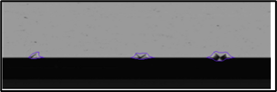
Figure 4: Chipping defects
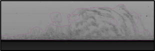
Figure 5: Staining defects
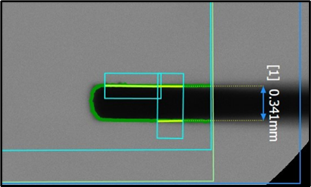
Figure 6: Wafer chamfer parameter measurement
Previously, Urespect has successively launched the first series of FTIR (Fourier Transform Infrared Spectroscopy)
measurement equipment for semiconductors in China (some models have received orders from overseas customers):
It is suitable for the Eos200/Eos300 film thickness measurement device for silicon-based epitaxial layers
It is suitable for silicon-based element concentration (B/P/F) measurement devices Eos200+/Eos300+
Through the optimized hardware design (updated infrared spectrometer technology) and the self-developed
algorithm, the Eos200L measurement equipment for the film thickness of the epitaxial layer and the film thickness
of the epitaxial buffer layer of silicon carbide is realized
Through an optimized hardware design (updated infrared spectrometer technology) in conjunction with the
self-developed Global Fitting Algo. ® Algorithm technology realizes silicon carbide multi-layer (≥ 3-layer) epitaxial
film thickness measurement equipment Eos200L+
Eos200T, a device for measuring C/O content in silicon materials
The Wafer Resistivity Measurement Equipment SICV200 Youruipu has achieved the goal of completely benchmarking the
test performance of foreign suppliers and the localization of the equipment supply chain. At the same time, targeted
innovation and development has been made for the industry pain points of metal residues and indentations after CV
measurement of silicon carbide epitaxial wafers, and successfully solved the pain points of the industry, and has received
orders from many customers.
For the SICD200 of silicon carbide substrate wafer dislocation and microtubule detection equipment, Urespec has realized
the full detection of the whole wafer for silicon carbide dislocation detection, and the equipment has received orders from
overseas customers.
The Eos200DSR device realizes the thickness measurement of the top layer of silicon redoped on SOI wafers. At the same
time, it can be used for silicon-based lithium niobate thickness, wafer back seal LTO thickness and photoresist thickness
measurement.
Founded in 2021, led by returnees who have been engaged in the semiconductor industry for a long time, and jointly
initiated and established by a senior domestic semiconductor front-end process measurement equipment technical
team, we are committed to creating high-quality semiconductor front-end measurement equipment.


 Added:
 Back to list