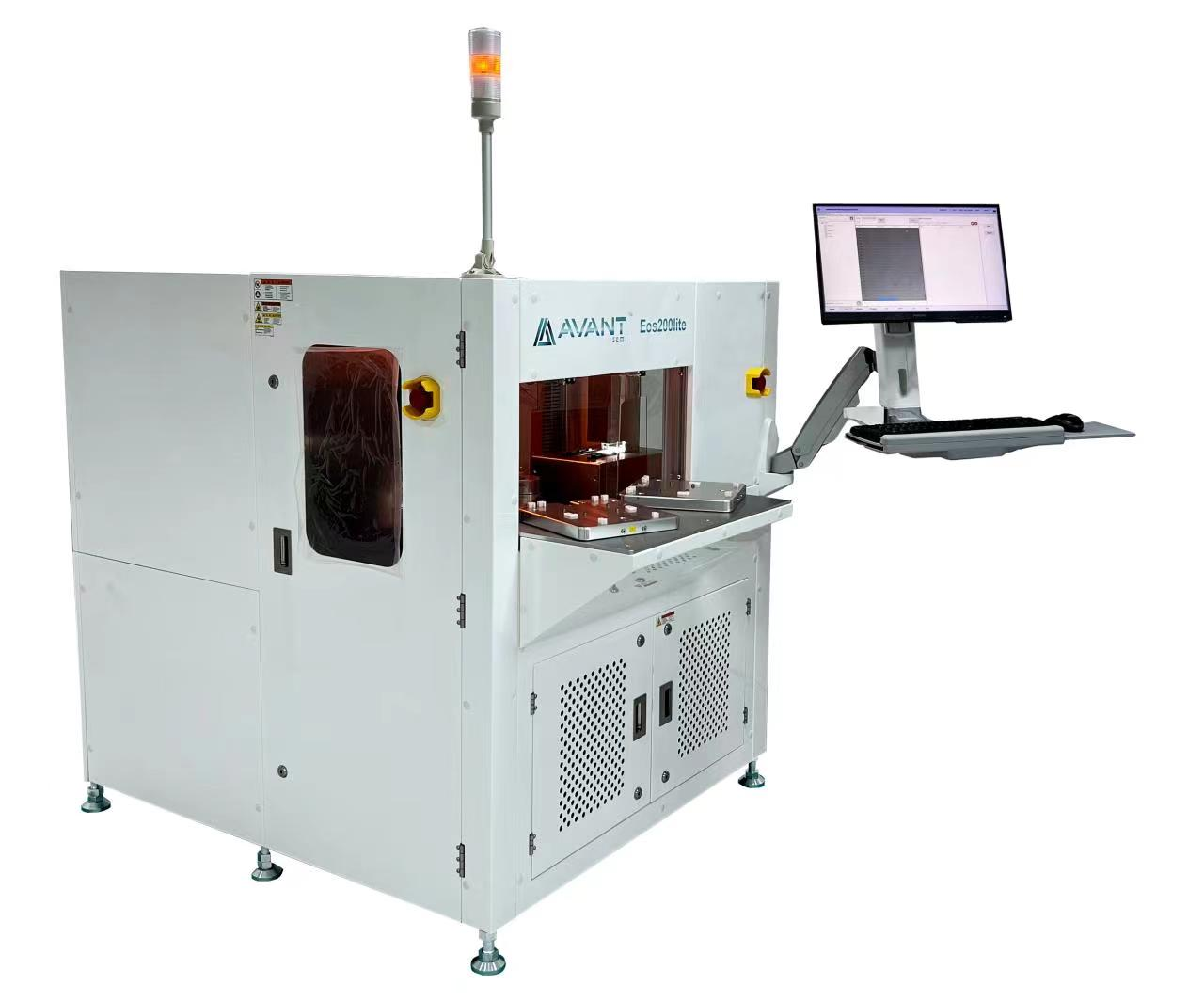

Industrial standard robot wafer transmission system with built-in
prealigner;
Modular design of optical units using mature Yourui spectral
Fourier infrared technology;
Air cooled infrared light sources, solid-state lasers, and
moisture-proof design can reduce maintenance costs (COO)
And extend the normal operation time of the equipment;
Equipped with a Yourui spectrum epitaxial film thickness
analysis system;
Customized algorithm for measuring the thickness of
silicon carbide epitaxial film;
Can measue SiC EPI buffer layer thickness;
Optimized design for streamlined compression, with
a smaller footprint;
Fully compliant with SECS/GEM standards, the SECS
interface supports local control operations,Remote
control operation of the host through the
HSMS/SECS-1 protocol;
The user-friendly client server architecture allows for
fast data collection and 2D or 3D imaging;
Has passed SEMI S2 certification;
Benefits
Contact-less measurement of epitaxial thickness by FTIR technique with very high operation throughput
Ability to determine epitaxial thickness on bulk or on patterned wafers such as silicon, SiC, GaAs, etc. It is also capable of measuring multiple grown epitaxial layers
Measurements are traceable to internal Golden Standards
Friendly user interface with convenient and fast recipe setup
Features
Ability to sort between source and destination cassettes
Patented Fixed-Reference-on-Chuck standard without the need for background wafer
Dual robot arms with stage design allows high stability and throughput
Service-free interferometer with air cooled IR source and solid-state laser design provides high stability and lower PM time and lower COO
Optical system utilizes ZnSe beam splitter and window with room temperature DTGS detector which does not require nitrogen purge for moisture protection, resulting in lowered COO
Ability to provide certain customization for system software upon customer special request