Following the successful launch of the wafer resistivity measurement equipment SICV200, Avant Semiconductor Equipment (Wuxi) Co., Ltd. (hereinafter referred to as "Avantsemi) has recently successfully delivered a thin film thickness measurement device Eos200DSR to the customer.
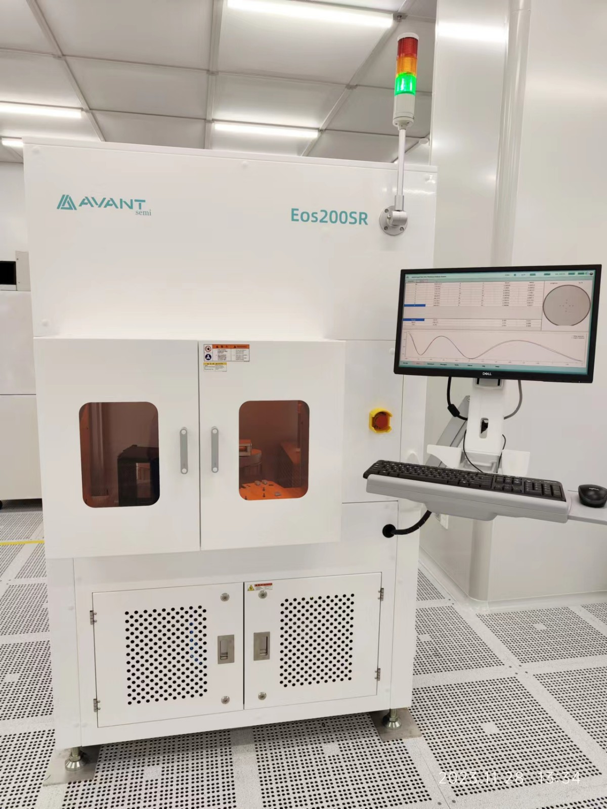
Figure 1: Eos200DSR in customer FAB
The Eos200DSR is a fully automated device compatible with 8/6 inch wafer sizes for measuring the thickness of multiple layers of different materials on the surface of SOI (Silicon-On-Insulator) wafers. One such application is the simultaneous measurement of silica (BOX) and a wide range of top layer silicon thickness on SOI wafers. The Eos200DSR can measure the thickness of the top layer of silicon from less than 1 micron to several hundred microns while measuring the BOX from tens of nanometers to several microns.
The device can also be applied to the requirements of thin film measurement of other materials, such as the emerging lithium niobate on silicon.
The Eos200DSR (6&8 inch wafer) and Eos300DSR (12 inch wafer) are fully SEMI compliant fully automated solutions that can be directly connected to the MES system of the customer's factory to achieve automated production.
Previously, Eurospec has successively launched a series of semiconductor-specific FTIR (Fourier Transform Infrared Spectroscopy) measurement equipment:
It is suitable for the Eos200 / Eos300 film thickness measurement device for silicon-based epitaxial layers
It is suitable for silicon-based element concentration (B/P/F) measurement devices Eos200+/Eos300+
Through the optimized hardware design (updated infrared spectrometer technology) and the
self-developed algorithm, the Eos200L is a measurement device for the film thickness of silicon
carbide (SiC) epitaxial layer and epitaxial buffer layer
Through the optimized hardware design (updated infrared spectrometer technology) and the self-developed
Global Fitting Algo.TM algorithm technology, the Eos 200L+ is a silicon carbide multilayer (≥ 3-layer)
epitaxial film thickness measurement device
Helios, a device for measuring C/O content in silicon.
The SICV200 wafer resistivity measurement equipment released by Urespec not only achieved the test
performance of completely benchmarking foreign suppliers, but also completed the localization goal of the
equipment supply chain.
The recently launched SICD200s/SICD200 inspection equipment for silicon carbide substrate dislocations
and microtubules introduces the line scan technology in the IC industry defect detection into the dislocation
and microtubule detection of silicon carbide substrates, compared with the traditional surface scanning
technology, the SICD series equipment can quickly realize the full scan of the entire wafer (the scanning
time of the whole wafer is ≤ 7 minutes), greatly improving the inspection efficiency of the client, and
ensuring the authenticity and reliability of the inspection results. Escort the quality of silicon carbide
substrate wafers.
Founded in 2021, led by returnees who have been engaged in the semiconductor industry for a long
time, and jointly initiated and established by the semiconductor front-end process measurement
equipment technical team, Uruipu is committed to creating high-quality semiconductor front-end
measurement equipment.


 Added:
 Back to list