Avant Semiconductor Equipment (Wuxi) Co., Ltd. (hereinafter referred to as "AVANTsemi") announced that the company has recently successfully launched a wafer resistivity measurement equipment SICV200, which will be delivered to customers for verification.
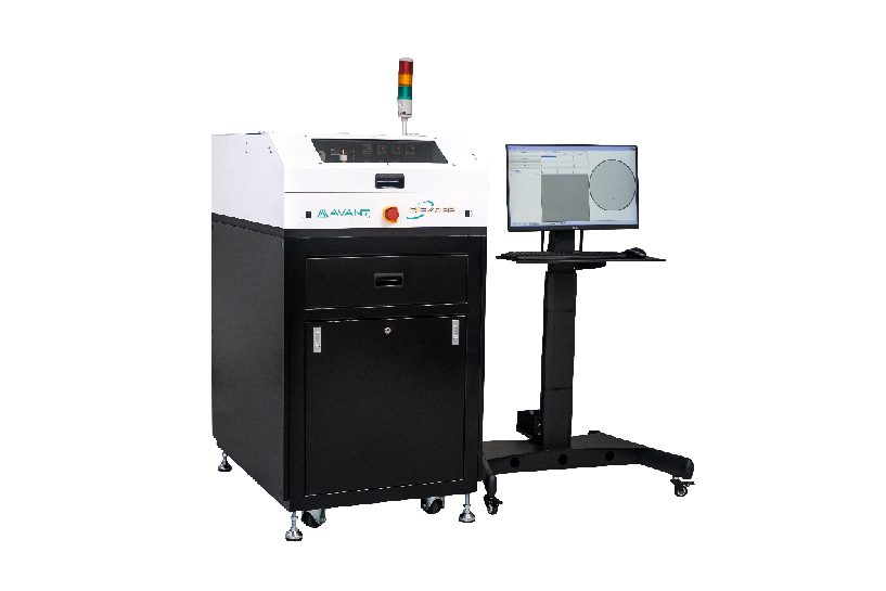
Figure1:SICV200 device
SICV200 is a semiconductor measurement device for measuring the resistivity of silicon wafers, doping concentration of silicon carbide or other semiconductor materials, and can support the analysis of CV characteristics at multiple frequencies for a variety of wafers of different sizes, including 12 inches. In terms of machine configuration, SICV200 has semi-automatic solutions of various sizes and fully automatic solutions in line with SEMI standards, which can be directly connected to the MES system of the customer's factory to achieve automated production.
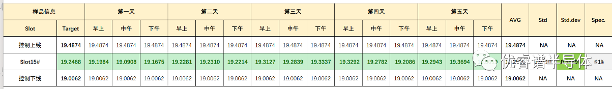 Table 1: SICV200 repeatability and long-term stability measurements
Dr. Tang Deming, general manager of Avantsemi, introduced that when homogeneous epitaxy is carried out on substrates,
carrier concentration is an important technical parameter. At present, the capacitive voltage (CV) method is commonly
used to measure the carrier concentration of the homogeneous epitaxial layer. This method can directly form a Schottky
barrier on the semiconductor to measure the carrier concentration of the epitaxial layer, and can also form a MOS capacitance
structure to monitor the CVD process, so as to effectively evaluate the carrier concentration and the quality of the epitaxial
layer in the manufacturing process of various semiconductor materials, and measure and analyze the semiconductor materials
conveniently and non-destructively, so as to provide basis and support for optimizing the epitaxial growth process.
In terms of technical solutions, in response to the suggestions and pain points put forward by customers in use, Uruipu
fully considers the independent and controllable supply chain and the needs of domestic substitution, improves and
optimizes the equipment accordingly, and makes progress in intellectual property rights and innovation.
Previously, Unispectrum has successively launched FTIR (Fourier Transform Infrared Spectroscopy) measurement equipment
for semiconductors:
It is suitable for the Eos200 / Eos300 film thickness measurement device for silicon-based epitaxial layers
It is suitable for silicon-based element concentration (B/P/F) measurement devices Eos200+/Eos300+
Through the optimized hardware design (updated infrared spectrometer technology) and the self-developed
algorithm, the Eos200L is a measurement device for the film thickness of silicon carbide (SiC) epitaxial layer
and epitaxial buffer layer.
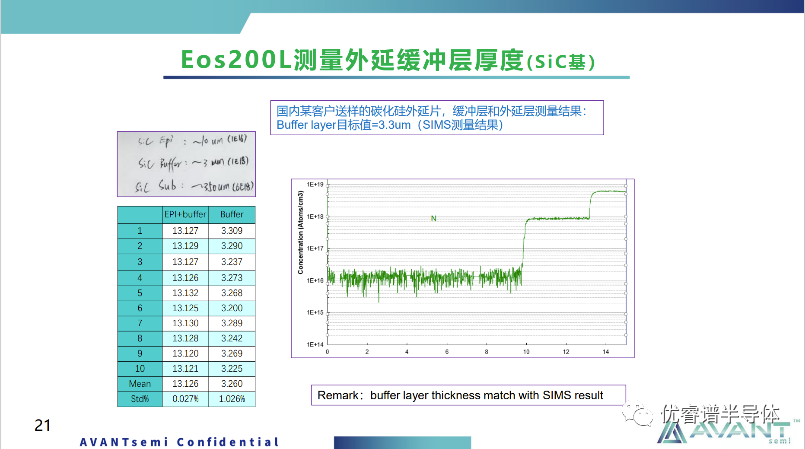
Figure 2: Eos200L measures the thickness of the silicon carbide epitaxial buffer layer
Through the optimized hardware design (updated infrared spectrometer technology) and the self-developed Global Fitting Algo.TM algorithm technology, the Eos 200L+ is a silicon carbide multilayer (≥ 3-layer) epitaxial film thickness measurement device.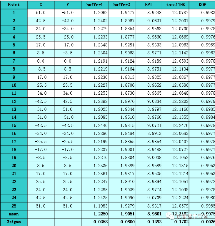
Figure 3: Eos200L+ measures the thickness of a silicon carbide multilayer epitaxial layer
Helios 200/300 measuring device for C/O content in silicon.
Silicon carbide substrate dislocation and microtubule inspection equipment SICD200s/SICD200, the equipment will be the IC industry defect detection in the line scan technology (Line Scan) into the silicon carbide substrate in the dislocation and microtubule detection, compared with the traditional surface scanning technology, the SICD series equipment can achieve the full scan of the entire wafer (full film scanning time ≤ 7 minutes), greatly improve the efficiency of client detection, while ensuring the authenticity and reliability of the inspection results, Escort the quality of silicon carbide substrate wafers.
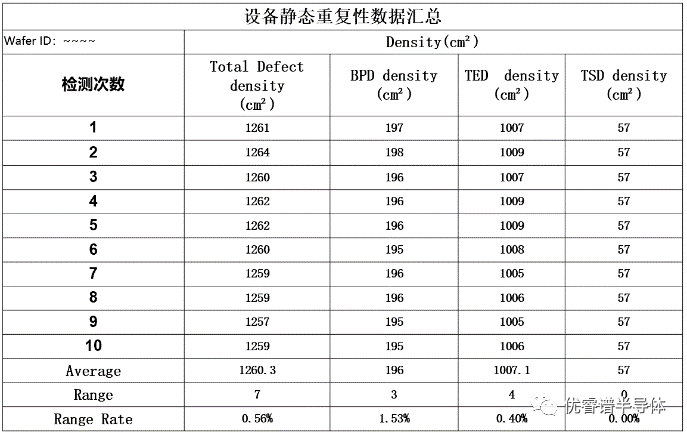
Figure 4: SICD200s device detects static repeatability
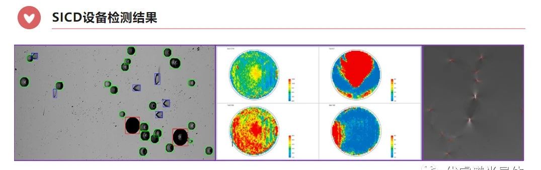
Figure 5: Illustration of SICD200s dislocation detection results
Founded in 2021, led by returnees who have been engaged in the semiconductor industry for a long time, and jointly initiated and established by the domestic semiconductor front-end process measurement equipment technical team, we are committed to creating high-quality semiconductor front-end measurement equipment.


 Added:
 Back to list