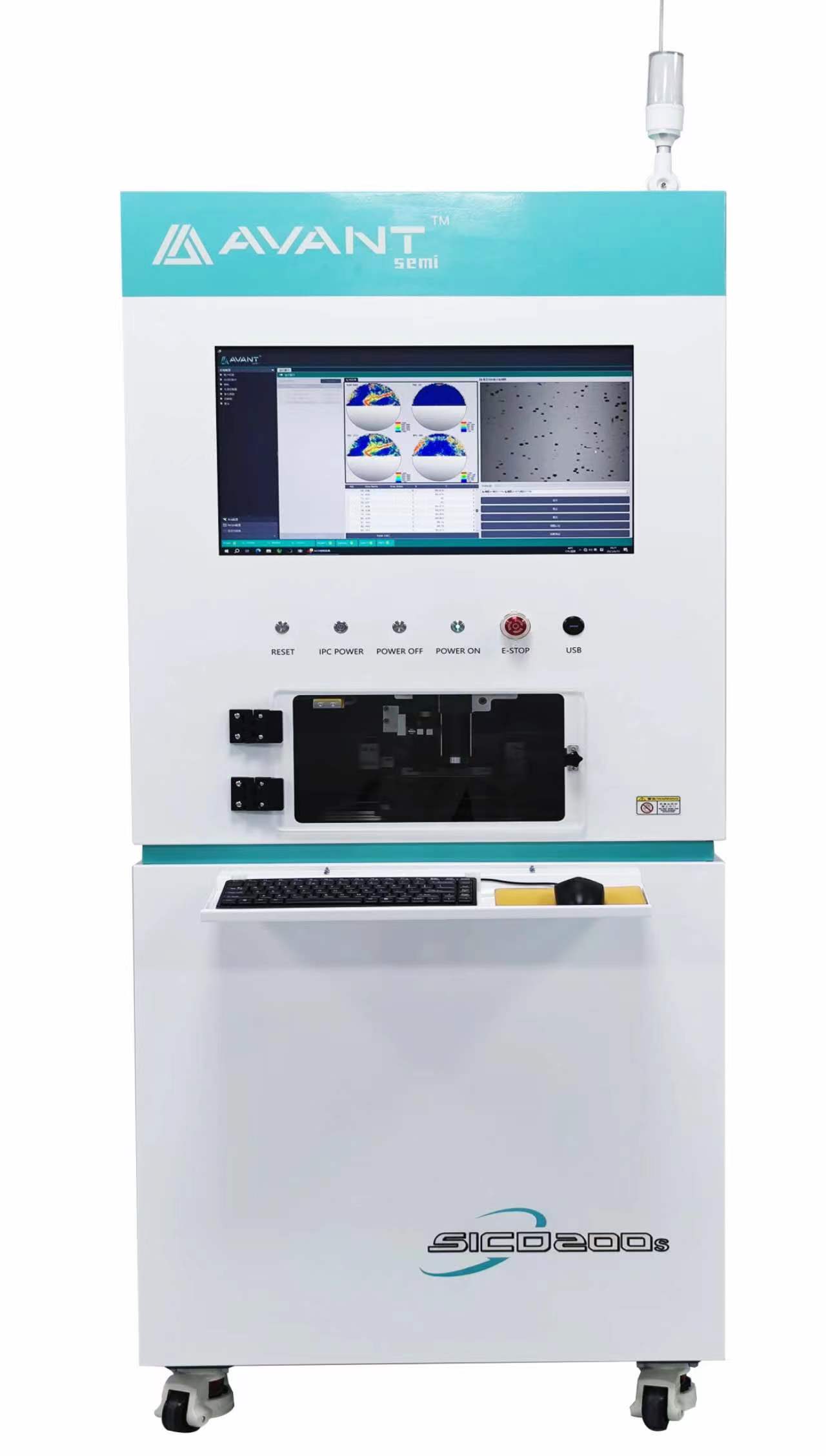
Recently, the company's SICD series of silicon carbide automatic optical error microtube detection equipment has been delivered to customers, which can be used for dislocation and microtube defect detection on silicon carbide substrates. According to Dr. Tang Deming, General Manager of Youruipu, SICD devices have increased their detection speed several times compared to similar devices in China
Established in 2021, Youruipu is committed to creating high-quality semiconductor front-end measurement
equipment.
Semiconductor measurement equipment is mainly used for defect detection and parameter measurement in
semiconductor manufacturing processes, and is widely used in the fields of silicon wafer manufacturing, chip
manufacturing, and advanced packaging, such as critical dimension measurement equipment, film thickness
measurement equipment, defect detection equipment, etc. The previous process measurement equipment has
exceeded the market size of tens of billions of dollars. And more advanced manufacturing processes have also
expanded the demand for measurement equipment, bringing more new market space for measurement
equipment.
Yourui Spectra has independently developed a semiconductor specific Fourier transform infrared spectroscopy
measurement equipment, which can be used to measure the thickness and uniformity of the epitaxial layer,
element concentration, silicon impurity content, and so on.
In terms of products, the Eos200Lite FTIR equipment of Yourui Spectrum can be used for measuring the thickness
and uniformity of the epitaxial layer of silicon carbide epitaxial wafers. Currently, it has received orders from
multiple top silicon carbide based epitaxial factories; Eos200/200+and Eos300/300+equipment for measuring
the thickness and element concentration of epitaxial layers on silicon based epitaxial wafers have also received
orders from multiple leading silicon based epitaxial factories and FAB factories.


 Added:
 Back to list